
The world of artificial intelligence is on the brink of a material revolution, a fundamental shift in how we construct the very foundations of our digital realm. We are moving beyond the conventional bottlenecks that have constrained computing for decades, particularly in the realm of AI. The core issue isn't a lack of raw processing power, but rather the sheer energy expenditure and inefficiencies involved in moving vast amounts of data.
The Invisible Barrier: The I/O Wall
For years, the pursuit of faster computing centered around Moore's Law—cramming more transistors onto smaller silicon chips. While processing power skyrocketed, the pathways connecting these mighty engines, the internal arteries of our systems, lagged significantly.
"Imagine standing at the edge of a cliff, staring down into a chasm. That chasm is filled with what we call the 'I/O Wall'—the invisible, yet impenetrable barrier that has been holding back the true potential of computing."
We've essentially built the equivalent of a supercar engine but connected it with flimsy fuel lines and a gearbox made of string. The engine's immense power becomes meaningless, bottlenecked by its incapable connections. This analogy perfectly encapsulates the current state of computing. Our magnificent silicon engines are shackled by copper wires rapidly becoming the Achilles' heel of high-performance computing, especially in AI.
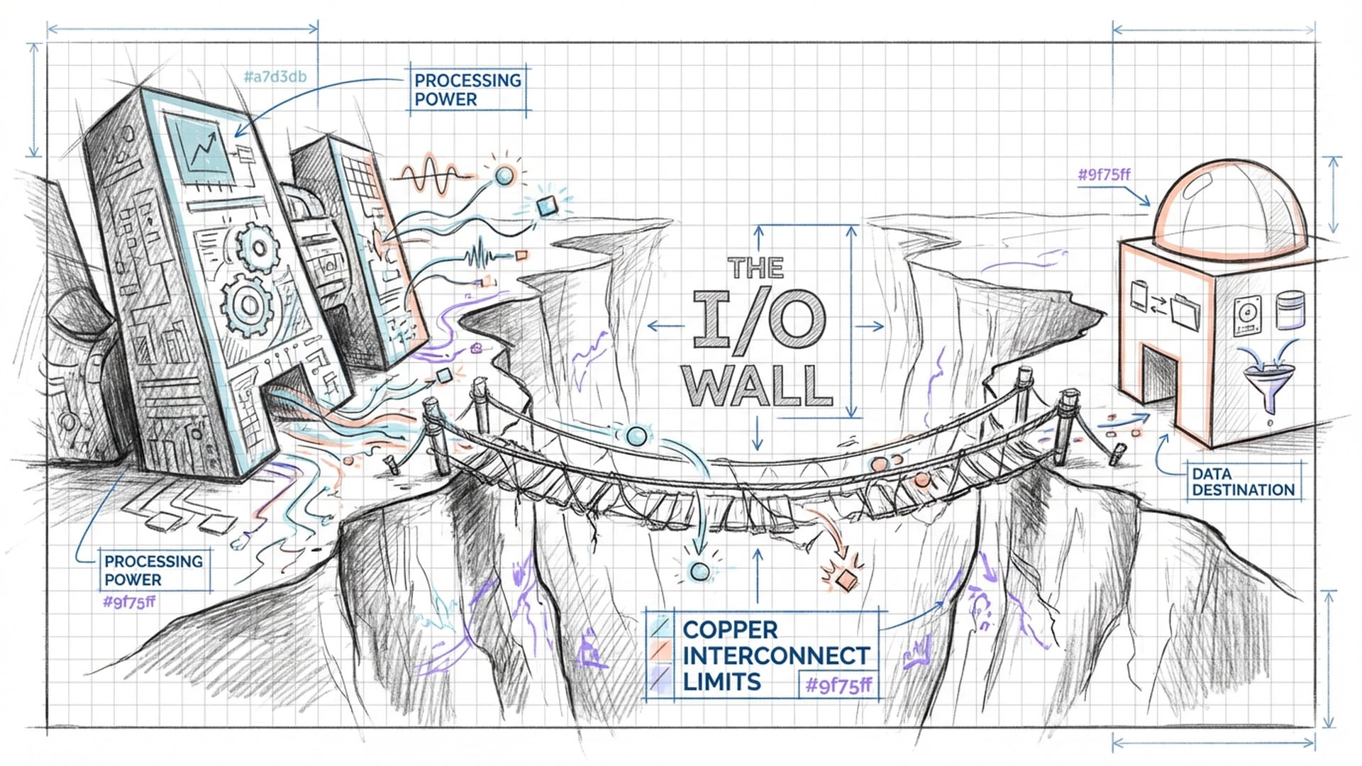
In the AI landscape, where models have expanded from millions to billions and now trillions of parameters, the energy required to merely shuffle data around chips, between chips, and across data centers has begun to overshadow the energy actually spent on processing that data. We've created an incredibly intelligent, yet incredibly sedentary behemoth, exhausted not from thinking, but from the immense effort of data retrieval.
The Dawn of a New Era: Silicon-Glass Hybrid Platform
On December 28th, 2025, a pivotal announcement shook the semiconductor world. Intel and TSMC unveiled a unified roadmap for what they termed the Silicon-Glass Hybrid Platform. This wasn't merely an incremental upgrade; it was a definitive declaration: the 'Copper Era' of high-performance computing was officially over.
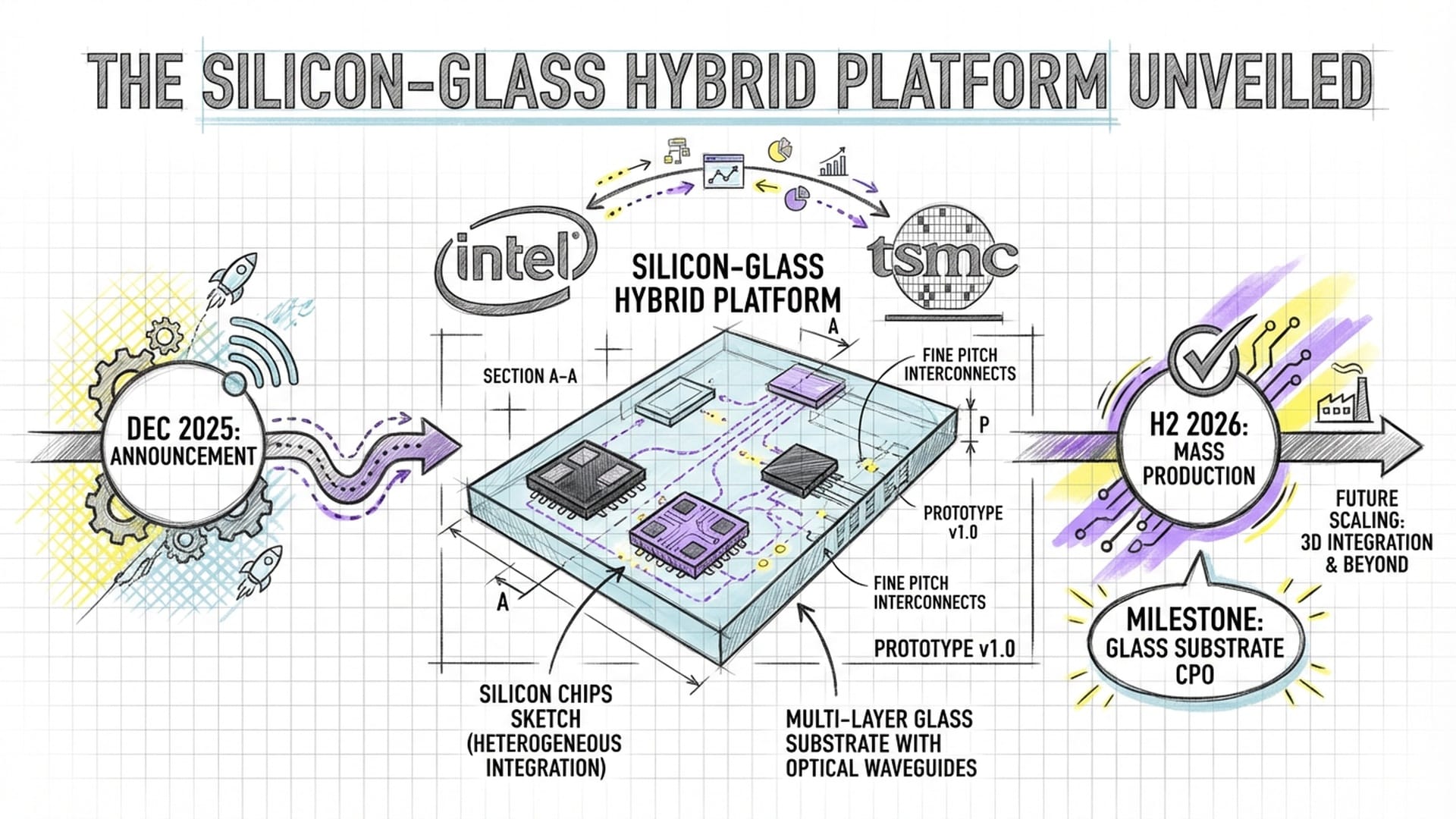
Their coordinated plan points to mass production, by the second half of 2026, of Glass Substrate-based Co-packaged Optics (CPO). The implications are profound, promising an eight-fold increase in bandwidth density, capable of moving over one hundred Terabits per second of data through a single package. Most critically, it promises a staggering forty percent reduction in the energy required to move each bit of that data.
This isn't just marketing hype; it's fundamental physics bending to our will, addressing the two invisible adversaries we've been fighting: signal integrity degradation and power density constraints. These aren't just engineering challenges; they are immutable limits imposed by physics on our ability to move electrons through copper.
The Limitations of Copper: Skin Effect and Dielectric Loss
For decades, our electronic highways relied on organic substrates—advanced, multi-layered circuit boards made mostly of fiberglass and resin—where data traveled through copper traces. While sufficient for a time, pushing speeds beyond 100 Gigabits per second (PAM4) into the 224 Gigabits per second (PAM4) territory revealed inherent physical limitations.
The Problem of Skin Effect
At high frequencies, electrical current flowing through copper wires doesn't utilize the entire wire. Instead, it's pushed to the outer surface, much like water flowing around the edges of a pipe. This phenomenon, known as the Skin Effect, dramatically reduces the effective cross-sectional area for current flow.
"Imagine trying to drive a super-fast car on a highway that suddenly shrinks to a bicycle path. That's the skin effect."
At 224 Gigabits per second, the resistance of that copper wire isn't just marginally higher; it's orders of magnitude greater than at lower frequencies.
The Challenge of Dielectric Loss
Adding to the complexity is Dielectric Loss. The organic materials encapsulating copper traces are not perfect insulators. At extremely high frequencies (exceeding 100 Gigahertz), the electromagnetic field causes tiny molecular dipoles within the resin to vibrate, absorbing electromagnetic energy and converting our precious signal into waste heat.
This insertion loss can consume three to four decibels per inch at 112 Gigahertz. A signal traveling just a few inches can degrade to the point of being indistinguishable from background noise, like a shout across a room fading to a whisper.
The DSP Tax and the Power Wall
These challenges culminate in what the industry calls the 224G limit. Electrical signals on organic substrates degrade so rapidly they can barely exit the chip package. To compensate, engineers employ massive Digital Signal Processors (DSPs) and retimers to constantly amplify and clean up these degraded signals. This comes at a huge cost: the DSP Tax.
"In today’s AI clusters, an astonishing thirty to forty percent of the total system power isn't going into the actual computation... No, it’s consumed by the I/O circuits, simply moving data between chips!"
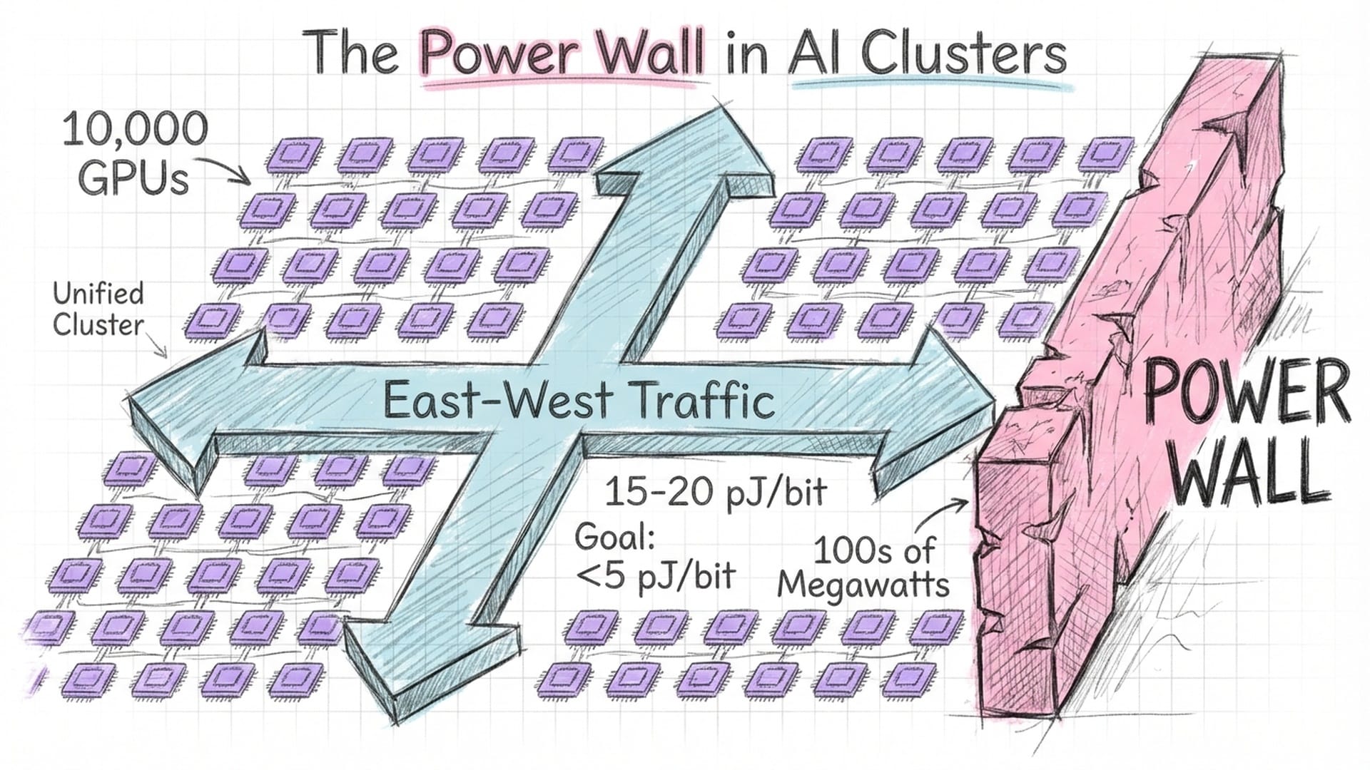
This power overhead inflates electricity bills and generates colossal amounts of waste heat, making thermal management a nightmare. This energy crisis is most acute in Generative AI. Training massive models requires thousands of GPUs working in perfect synchronicity, leading to immense East-West data traffic. With traditional interconnects, data movement costs 15-20 picojoules per bit. Multiplied across the scale of these clusters, this rockets power consumption to hundreds of megawatts, creating an insurmountable Power Wall. Data centers face hard caps on power consumption and heat dissipation, grinding AI scaling to a halt.
Why Glass? The Radical Material Swap
The Intel-TSMC breakthrough directly addresses this power wall by aiming to slash data movement energy costs to less than five picojoules per bit. This isn't a small improvement; it's a three-fold increase in energy efficiency, unlocking the ability to train far larger models within existing power envelopes.
Glass isn't merely a replacement; it's a platform shift, enabling entirely new manufacturing capabilities and performance metrics.
Dimensional Stability and Precision
Glass is incredibly stiff and flat, unlike inherently flexible organic substrates that warp. As chip packages grow, warpage becomes a significant yield-killing defect. Glass solves this by maintaining its shape under extreme thermal stresses.
This extreme flatness offers two key advantages:
- Lithography precision: The pristine flatness enables
panel-level lithographywith high depth-of-focus, allowing a ten-fold increase in interconnect density compared to organic substrates. This means tighter chiplet packing and more I/O pathways. - Warpage control: Glass substrates exhibit 50% less pattern distortion and significantly reduced warpage, critical for next-gen GPUs like NVIDIA’s Rubin and AMD’s MI400, which integrate dozens of silicon dies.
Through-Glass Vias (TGVs): Superhighways for Data
The true magic lies in Through-Glass Vias (TGVs). These are microscopic vertical tunnels, drilled through the glass core and filled with copper. Glass, being an outstanding electrical insulator, minimizes signal attenuation in TGVs, preserving signal integrity at hundreds of Gigahertz, supporting 224G and even future 448G signaling standards without the insatiable power demands of copper.
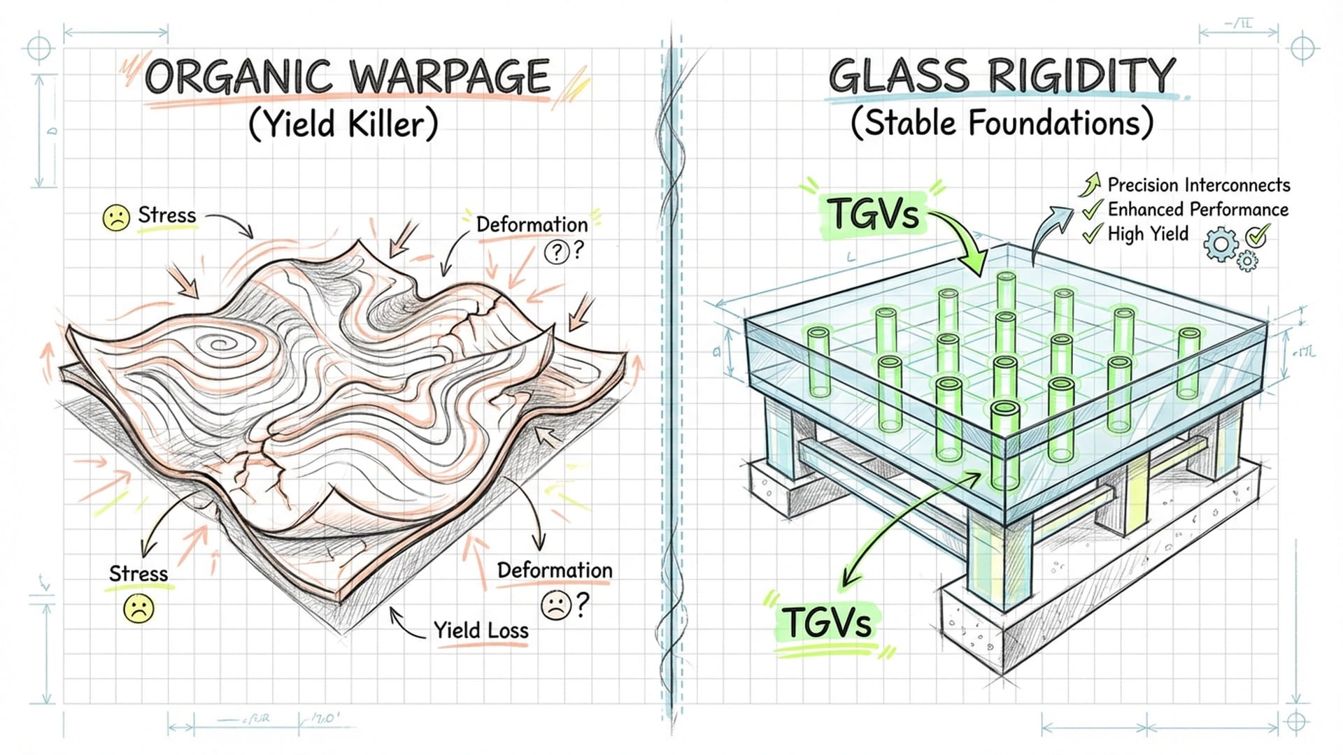
TGVs can be packed much closer together than traditional through-hole vias, enabling massive, parallel I/O. This solves the beachfront problem, where a chip lacks sufficient edge space for data routing. High-density TGV arrays allow signals to escape vertically from anywhere under the chip, not just its perimeter.
"Imagine a skyscraper where you don't just have elevators on the outside, but elevators punching straight through the middle of every floor. That's the power of TGVs."
Co-Packaged Optics (CPO): The Ultimate Velocity
While glass provides the stable foundation, the velocity comes from Co-Packaged Optics (CPO)—the third and most radical phase of optical evolution in the data center.
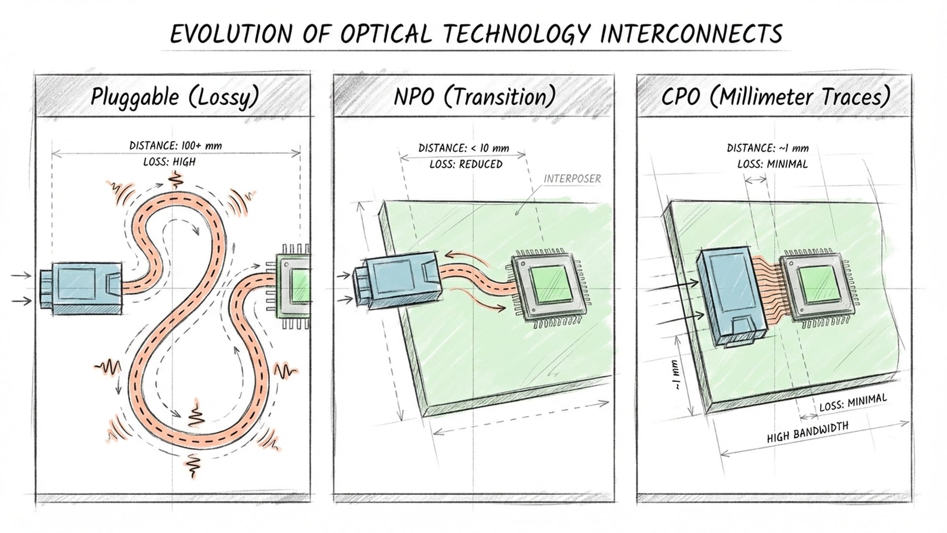
The Evolution of Optics
- Pluggable Optics: Electrical signals travel inches across circuit boards to a front-panel connector, where they convert to light. This long electrical path incurs massive loss, demanding power-hungry DSPs. It's like running a marathon before getting to the starting line.
- Near-Packaged Optics (NPO): Optical modules moved onto the main circuit board, shortening the electrical trace but still relying on separate modules. A transitional, complex step.
- Co-Packaged Optics (CPO): The optical engine moves inside the package, sitting on the same (
glass) substrate as the GPU or switch ASIC. The electrical path is shortened from inches to millimeters, eliminating the need for expensive, power-guzzling retimers and DSPs. This architecture alone can break the five picojoule per bit energy barrier.
TSMC's COUPE (Compact Universal Photonic Engine) is a specific implementation of CPO, a 3D-stacked photonic integrated circuit platform designed for maximum bandwidth density and energy efficiency. It stacks the Electronic Integrated Circuit (EIC) directly atop the Photonic Integrated Circuit (PIC) using bumpless hybrid bonding, creating an ultralow impedance connection.
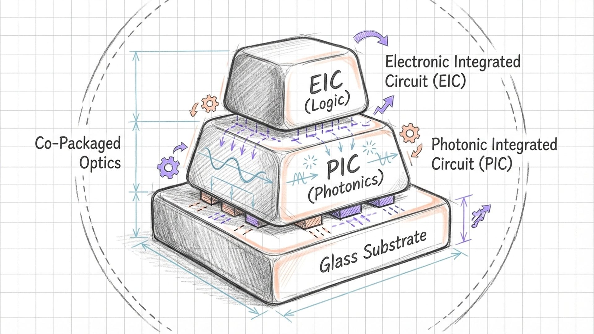
The integrated COUPE block mounts onto the glass substrate, utilizing glass's superior optical properties for advanced optical coupling. TSMC projects that COUPE can reduce laser power consumption by over 40% and increase bandwidth density by a phenomenal twenty-three times compared to traditional solutions.
A Hybrid Ecosystem and the End of the LPO Debate
The Intel-TSMC announcement highlights a hybrid approach, combining Intel's expertise in glass core material science with TSMC's prowess in 3D silicon stacking. This standardized ecosystem allows for interoperability, where specialist glass suppliers (like Absolics or Corning) can provide robust substrates for TSMC-fabricated compute dies communicating with Broadcom optical engines, all through a unified protocol.
This joint announcement also puts a decisive end to the Pluggable versus CPO debate that characterized the 2024-2025 investment landscape. Linear Drive Pluggable Optics (LPO), a transitional technology that removed DSPs from pluggable modules, is officially a stopgap. While LPO offered power savings, its reliance on incredibly clean channels and its limited reach at 224G speeds made it unsuitable for large-scale AI clusters.
"LPO simply cannot match CPO’s bandwidth density. A CPO package can offer one hundred Terabits per second of edge bandwidth. Achieving that with traditional pluggable modules would demand a front panel larger than the server rack itself."
CPO enables radix (connectivity scales) impossible with front-panel plugs. Major players like NVIDIA (Rubin) and AMD (MI400) are already designing their 2026-2027 roadmaps with CPO in mind. The sheer compute density, projected to exceed 120 kilowatts per rack, leaves no physical room for thousands of front-panel cables. The optics must move inside the package for crucial space, cooling, and power delivery. This effectively deprecates LPO for flagship AI designs post-2026.
The New Supply Chain: Glass Barons and CPO Engine Builders
This shift to glass creates an entirely new tier in the semiconductor supply chain, shifting focus from front-end (transistor scaling) to back-end (advanced packaging and interconnects). Value is migrating from the wafer to the package.
The 'Glass Barons':
- Absolics: Targeting mass production by late 2025.
- Corning: Leveraging its
fusion drawprocess for ultra-flat panels, projecting a $10 billion glass substrate market by 2026. - Schott: High-precision supplier for RF, 5G, and AI with ultra-low dielectric loss glass.
The 'CPO Engine Builders':
- Broadcom: Market leader, already on its second generation of
BaillyCPO switches. - Marvell: Focused on
cloud-optimizedCPO for hyperscalers. - Lightmatter: A disruptor with
Passagetechnology, building programmable photonic interconnects, envisioning a future where the network and computer are indistinguishable.
Standardizing the Future: UCIe and OIF
The success of this hybrid ecosystem hinges on two key standards bodies:
- UCIe (Universal Chiplet Interconnect Express): The protocol enabling a GPU chiplet to talk to an Optical Engine chiplet on the glass substrate. The Intel-TSMC announcement likely includes a
UCIe-Optical extension, standardizing the physical layer for optical I/O. - OIF (Optical Internetworking Forum): Addressing the challenge of laser degradation in high heat. The OIF is defining the
ELSFP(External Laser Small Form Factor Pluggable) standard, allowing the laser source to remain external and pluggable. Thisremote light sourceapproach ensures serviceability and reliability, as a technician can replace a $500 laser module instead of a $50,000 GPU package if the laser fails.
Investment Thesis: The Glass Era Is Here
The Intel-TSMC milestone is perfectly timed to support the next generation of AI flagships. NVIDIA's 'Rubin' architecture and AMD's 'Helios' platform are being designed for this Glass Era. NVIDIA's NVLink 6.0 is expected to transition to optical for rack-scale communication, with the glass substrate as the physical carrier, enabling a flat network topology where every GPU communicates with minimal latency.
The CPO market is projected to grow at a Compound Annual Growth Rate (CAGR) of 37-46% from 2026 to 2036, exceeding $20 billion by 2036. The glass substrate market alone is estimated to reach $10-12 billion by 2035.
Who wins?
- Substrate/Material Suppliers: Corning and Absolics, with their proprietary glass formulations.
- CPO Leaders: Broadcom and Marvell, dominating the DSP and Optical Engine market.
- Advanced Packaging Foundries: TSMC, retaining its integration crown, and Intel, with a new opportunity to monetize its glass expertise as a merchant foundry.
Who's at risk?
- Traditional PCB Makers: Those relying solely on organic substrates for high-end markets will see commoditization.
- Legacy Pluggable Optics Vendors: Slow to pivot to CPO engines, they risk obsolescence in the AI server market.
The joint 2026 milestone from Intel and TSMC is a collective acknowledgment that copper has reached its physical limit. The transition to the Silicon-Glass Hybrid Platform solves the most pressing bottleneck of the AI era: the prohibitive energy cost of moving data. By 2027, the standard AI Superchip will be a complex, 3D-stacked metropolis of compute and memory, resting on a transparent sheet of glass, communicating through pulses of light.
The future of AI infrastructure is transparent, rigid, and optical. The Glass Era has not just begun; it's already here, demanding we adapt, innovate, and look at the world through a new, clearer lens.